Current Research
Vertical GaN p-i-n Diodes on Si
|
Fully- and quasi-vertical GaN-on-Si p-i-n diodes were grown and fabricated. A record high Baliga figure of merit of 304 and 152 MW/cm2 is reported for fully-and quasi-vertical GaN-on-Si p-i-n diodes, respectively. A comprehensive comparison has been made between the two kinds of diodes in regard ON-resistance, breakdown voltage, and switching performance. An ultralow differential ON-resistance of 0.5 and 1.0 mOhm•cm2 has been demonstrated for quasi- and fully-vertical diodes with a diameter of 60μm at 3kA/cm2. Current crowding effect in the n-GaN was a dominant factor of RON, especially for large size quasi-vertical diodes at high current density. A high Vbr of 390 V has been demonstrated for the two types of device structures, regardless of device diameters. The same breakdown voltage and low off-state leakage indicated the reliability of fully-vertical device fabrication that reflects intrinsic properties of the grown epilayers. The two kinds of diodes share similar switching performance, which is much superior to a commercial fast-recovery Si diode as a reference. The device characteristics show promising potential of both fully- and quasi-vertical diodes for low-cost high-power applications.
Fig. 1. Schematic of (a) epitaxial structure of p-i-n diodes grown on (111) Si, (b) quasi-vertical p-i-n diodes on original substrate (with no vertical overlap of two electrodes), and (c) fully-vertical p-i-n diodes with GaN thin film transferred onto a (100)Si receiver (with vertical overlap of two electrodes).
Fig. 2. (a)–(e) Forward bias I–V characteristics of fully- and quasi-vertical diodes with diode mesa diameter ranging from 60 to 300 μm (black symbols); the corresponding specific ON-resistance for all the current level is also plotted (blue symbols). Very low specific RON less than 1 mΩ•cm2 could be readily observed for fully-vertical diodes at high current injection. (f) Ideality factor for two kinds of diodes with a diameter of 150 μm.
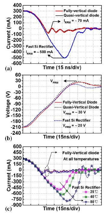
Fig. 3. (a) Current waveforms during reverse recovery and (b) voltage waveforms during forward recovery of the fully-, quasi-vertical p-i-n GaN diode, and commercial fast Si rectifier (Fairchild, UF4004), respectively. (c) Current waveforms during reverse recovery of fully-vertical p-i-n GaN diode and Si rectifier at different temperatures. |